flash_driver.c File Reference
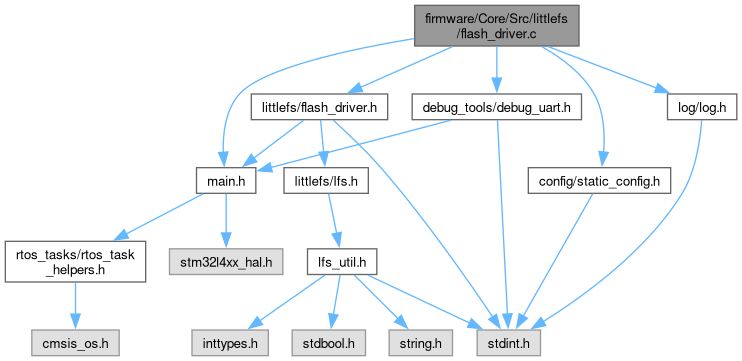
Include dependency graph for flash_driver.c:
Functions | |
| static FLASH_error_enum_t | FLASH_disable_block_lock (uint8_t chip_number) |
| Disable the block lock feature of the flash chip, which is enabled by default after a power cycle. | |
| static FLASH_error_enum_t | FLASH_write_enable (uint8_t chip_number) |
| static FLASH_error_enum_t | FLASH_write_disable (uint8_t chip_number) |
| static FLASH_error_enum_t | FLASH_wait_until_ready (uint8_t chip_number) |
| Wait until the flash chip is ready for the next command. | |
| FLASH_error_enum_t | FLASH_init (uint8_t chip_number) |
| FLASH_error_enum_t | FLASH_erase_block (uint8_t chip_number, FLASH_Physical_Address_t address) |
| FLASH_error_enum_t | FLASH_program_page (uint8_t chip_number, FLASH_Physical_Address_t address, uint8_t *data, uint32_t data_len) |
| FLASH_error_enum_t | FLASH_read_page (uint8_t chip_number, FLASH_Physical_Address_t address, uint8_t *rx_buffer, uint32_t rx_buffer_size) |
| FLASH_error_enum_t | FLASH_is_reachable (uint8_t chip_number) |
| FLASH_error_enum_t | FLASH_reset (uint8_t chip_number) |
| FLASH_error_enum_t | FLASH_read_status_register (uint8_t chip_number, uint8_t *response) |
| void | FLASH_enable_then_disable_chip_select (uint8_t chip_number) |
| Here for testing purposes. | |
Function Documentation
◆ FLASH_disable_block_lock()
|
static |
Disable the block lock feature of the flash chip, which is enabled by default after a power cycle.
Here is the call graph for this function:

Here is the caller graph for this function:

◆ FLASH_enable_then_disable_chip_select()
| void FLASH_enable_then_disable_chip_select | ( | uint8_t | chip_number | ) |
Here for testing purposes.
- Parameters
-
chip_number the chip select line to enable.
Here is the call graph for this function:

Here is the caller graph for this function:
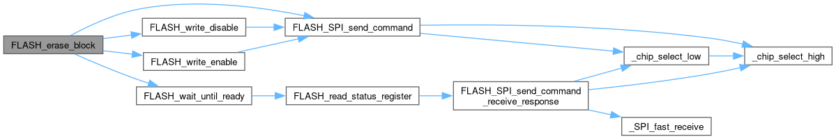
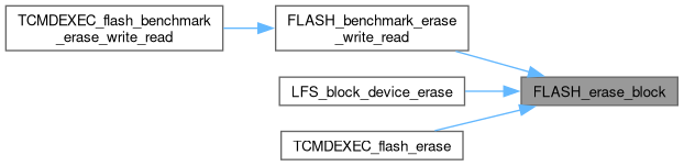
◆ FLASH_erase_block()
| FLASH_error_enum_t FLASH_erase_block | ( | uint8_t | chip_number, |
| FLASH_Physical_Address_t | address ) |
Here is the call graph for this function:
Here is the caller graph for this function:
◆ FLASH_init()
| FLASH_error_enum_t FLASH_init | ( | uint8_t | chip_number | ) |
Here is the call graph for this function:

Here is the caller graph for this function:

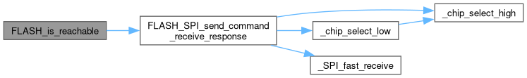
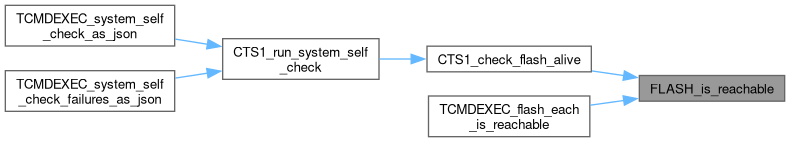
◆ FLASH_is_reachable()
| FLASH_error_enum_t FLASH_is_reachable | ( | uint8_t | chip_number | ) |
Here is the call graph for this function:
Here is the caller graph for this function:
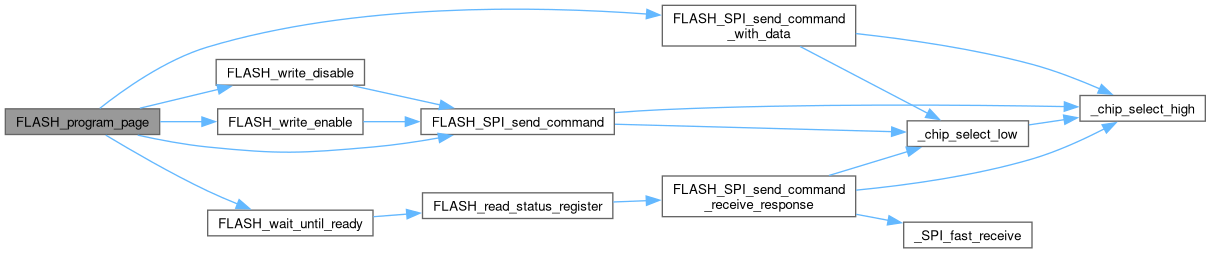
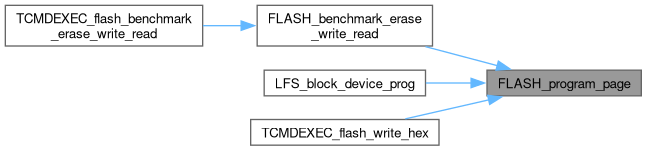
◆ FLASH_program_page()
| FLASH_error_enum_t FLASH_program_page | ( | uint8_t | chip_number, |
| FLASH_Physical_Address_t | address, | ||
| uint8_t * | data, | ||
| uint32_t | data_len ) |
Here is the call graph for this function:
Here is the caller graph for this function:
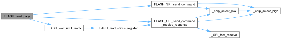
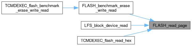
◆ FLASH_read_page()
| FLASH_error_enum_t FLASH_read_page | ( | uint8_t | chip_number, |
| FLASH_Physical_Address_t | address, | ||
| uint8_t * | rx_buffer, | ||
| uint32_t | rx_buffer_size ) |
Here is the call graph for this function:
Here is the caller graph for this function:
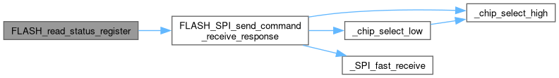
◆ FLASH_read_status_register()
| FLASH_error_enum_t FLASH_read_status_register | ( | uint8_t | chip_number, |
| uint8_t * | response ) |
Here is the call graph for this function:
Here is the caller graph for this function:
◆ FLASH_reset()
| FLASH_error_enum_t FLASH_reset | ( | uint8_t | chip_number | ) |
Here is the call graph for this function:

Here is the caller graph for this function:

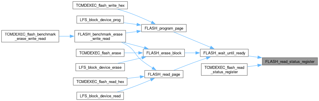
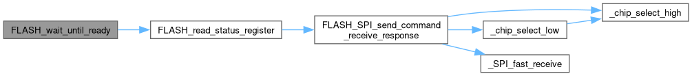
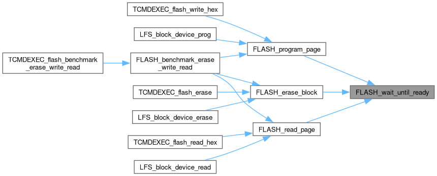
◆ FLASH_wait_until_ready()
|
static |
Wait until the flash chip is ready for the next command.
- Parameters
-
chip_number the chip select line to enable.
- Returns
- FLASH_ERR_OK on success, or an error code on failure.
Here is the call graph for this function:
Here is the caller graph for this function:
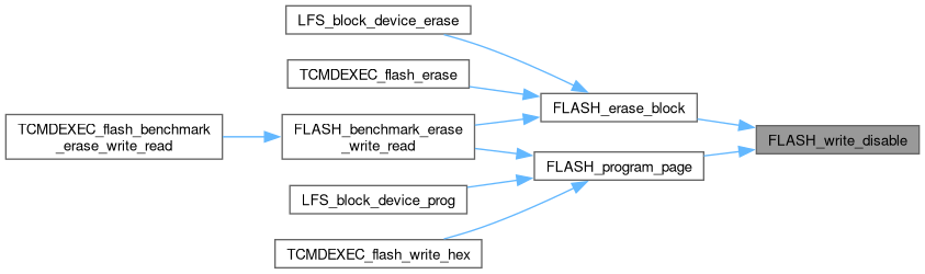
◆ FLASH_write_disable()
|
static |
Here is the call graph for this function:

Here is the caller graph for this function:
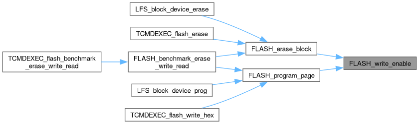
◆ FLASH_write_enable()
|
static |
Here is the call graph for this function:

Here is the caller graph for this function:
Generated by